
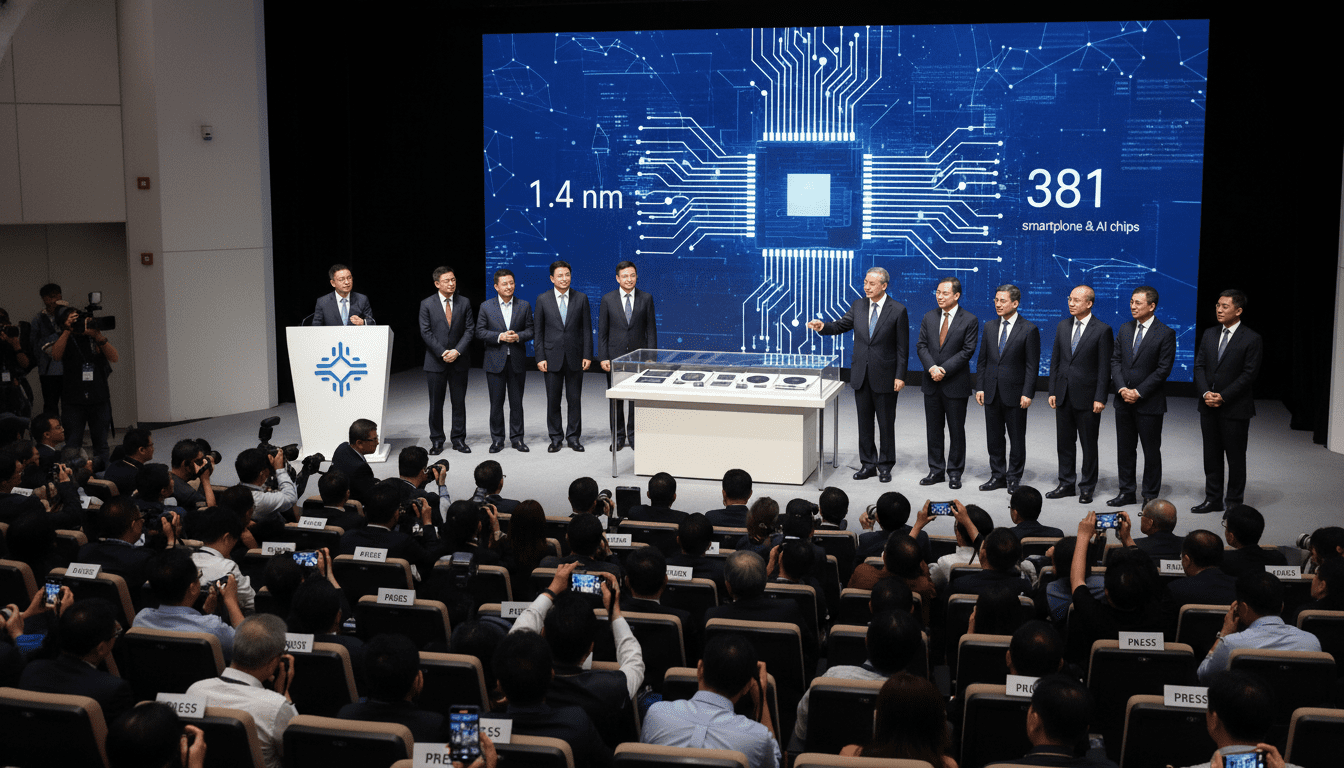
Huawei 1.4nm chip push: company reports 381 in-house designs amid industry scrutiny
Huawei says it designed 381 chips and is pursuing a 1.4-nanometer chip process; industry watchers await independent benchmarks and manufacturing clarity.
Huawei said it has designed and put into production 381 chips over the past six years, and the company is positioning a 1.4nm chip development as a future leadership goal. The announcement highlights Huawei’s push into advanced semiconductor design for smartphones and artificial intelligence, but independent performance data has not been made public. Analysts say a functioning 1.4-nanometer process would represent a major technical milestone if achieved at scale before the end of the decade. Market participants will be watching for third-party benchmarks and manufacturing details to verify the claims.
Company disclosure on chip designs
Huawei reported that its internal teams have produced 381 chips following the same design principles in the last six years. The company framed the disclosure as evidence of sustained investment in silicon for mobile devices and AI workloads.
The announcement did not include independent performance metrics or full technical specifications for those chips. Without external benchmarks, vendors, developers and customers lack objective data to compare Huawei’s designs against established rivals.
Technical ambition for a 1.4-nanometer process
Huawei’s reference to a 1.4-nanometer chip reflects an industry conversation about next-generation process nodes. A 1.4nm process, if realized commercially, would push transistor densities and energy efficiency beyond current mainstream nodes.
Engineering a 1.4nm node requires extreme ultraviolet lithography, advanced materials and tight process control, all of which raise questions about yields and production cost. Industry observers note that technology readiness, access to manufacturing partners and equipment are decisive factors that determine whether a claimed node becomes a market reality.
Industry expectations and competitive landscape
Semiconductor foundries and chipmakers have signaled in recent years that nodes below 2nm are the next frontier, with some expecting sub-2nm processes to emerge toward the end of this decade. Huawei’s statement places it within that broader competitive trajectory but does not establish where its designs sit relative to those being developed by specialized foundries.
Major foundries and chipmakers have long led the capital-intensive work of process shrink and packaging innovations. Huawei’s progress in chip design may give it greater product control, but commercial leadership at the 1.4nm level would likely require close collaboration with advanced fabs and equipment suppliers.
Manufacturing and supply chain challenges
Scaling a 1.4nm manufacturing process depends on a complex global supply chain, including lithography, wafer processing and packaging suppliers. Access to cutting-edge tools and materials, as well as stable supplier relationships, are essential to move from prototype to mass production.
Yield improvement and quality assurance at such nodes are often measured in months or years of iterative process work, which can be costly and technically demanding. Observers say the timeline for broad adoption will hinge on whether partners can deliver the necessary fabrication capacity and whether yields reach commercially viable levels.
Potential impact on smartphones and AI hardware
If Huawei succeeds in deploying designs that leverage a genuine 1.4nm process, the most immediate effects would likely be improved energy efficiency and higher on-chip performance for both smartphones and AI accelerators. Smaller nodes can enable denser logic, faster clocks and lower power consumption, which are valuable for mobile devices and edge AI applications.
Still, practical gains depend on system integration, software optimization and thermal management, so raw node size alone does not guarantee superior end-user experience. Without independent benchmarks or disclosed silicon samples, customers and OEMs will likely remain cautious about upgrading product roadmaps based solely on the claim.
Huawei’s announcement underscores its intent to deepen control over chip design for smartphones and AI, but it leaves key verification steps incomplete. Independent testing, clearer timelines and evidence of manufacturing partnerships will be central to determining whether the company’s 1.4nm ambitions translate into industry-leading products.
Observers say the semiconductor sector is entering a phase where design prowess must be matched by manufacturing credibility to influence market rankings. The coming months and years will reveal whether Huawei’s internal chip portfolio and its 1.4nm aspirations can withstand technical scrutiny and the demands of large-scale production.
